

FPGA Carrier Board
Signal Processing — FPGA Carrier
FPGA Carrier Board
The FPGA Carrier Card is the main processing node of the digital signal generation chain. It processes DTK/IQ data coming from the SBC via PCIe in real time and provides a high-speed JESD link to the AD9082 MxFE card over FMC+. It operates as a waveform engine in electronic warfare, radar, and communication applications.
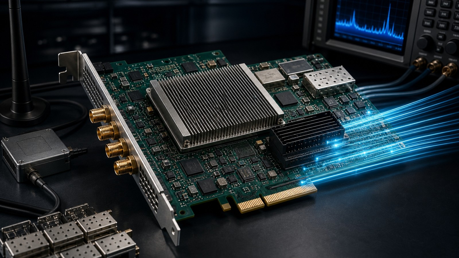
- SoC:Zynq UltraScale+ MPSoC
- FMC+:VITA 57.4
- Fabric:PCIe Gen3
- Serial Link:GTY 32 Gbps
Processor and Memory
| Feature | Value / Description |
|---|---|
| FPGA / SoC | Xilinx Zynq UltraScale+ MPSoC — ZU11EG / ZU17EG / ZU19EG |
| PS Processors | ARM Cortex-A53 (application processor) + ARM Cortex-R5 (real-time) |
| PS Memory | 4 GB DDR4 ECC |
| PL Memory | 8 GB DDR4 ECC |
| Flash | 2 GB QSPI Boot Flash |
| Security | TPM + encrypted FPGA bitstream + IPMC |
Interfaces
| Feature | Value / Description |
|---|---|
| FMC+ (VITA 57.4) | 12× GTY @ 32 Gbps, 12× GTH @ 16 Gbps, 160 I/O (80 LVDS) |
| VPX P0 | Power, IPMI/IPMB, I2C, JTAG, management signals |
| VPX P1 | PCIe Gen3 x4, 10GBASE-KR, REF_CLK, SYS_REF |
| VPX P2 | VITA 67.3C RF coax option |
| FMC+ Clock | DVC_CLK, SYSREF — DAC/ADC synchronization |
Technical specifications
Waveform engine advantages
Provides real-time DTK/IQ processing and JESD connectivity in electronic warfare, radar, and communication applications.
- Zynq UltraScale+ MPSoC
- PCIe Gen3 x4 VPX interface
- FMC+ VITA 57.4 high-speed serial links
- TPM and encrypted bitstream
Conclusion
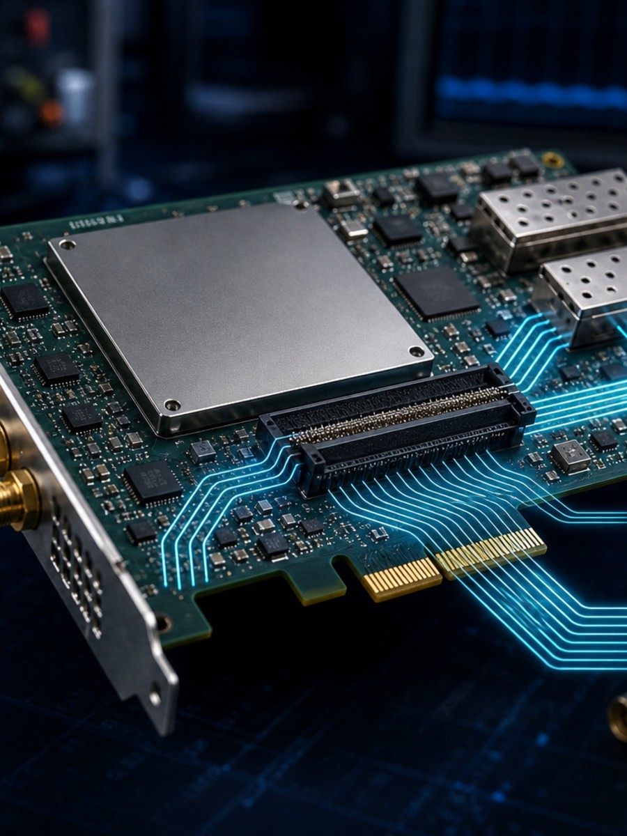
Modular signal generation infrastructure
Together with the AD9082 MxFE card, the FPGA Carrier Card forms the main processing node of a fully modular digital signal generator solution.