

FPGA + ADC/DAC
Signal Processing — FPGA + ADC/DAC
FPGA + ADC/DAC
The ADC/DAC-based FPGA Signal Generator is a module pair consisting of two cards. Digital signal processing and high-speed data bus, together with the analog/RF output chain, are combined over FMC+ interconnect.
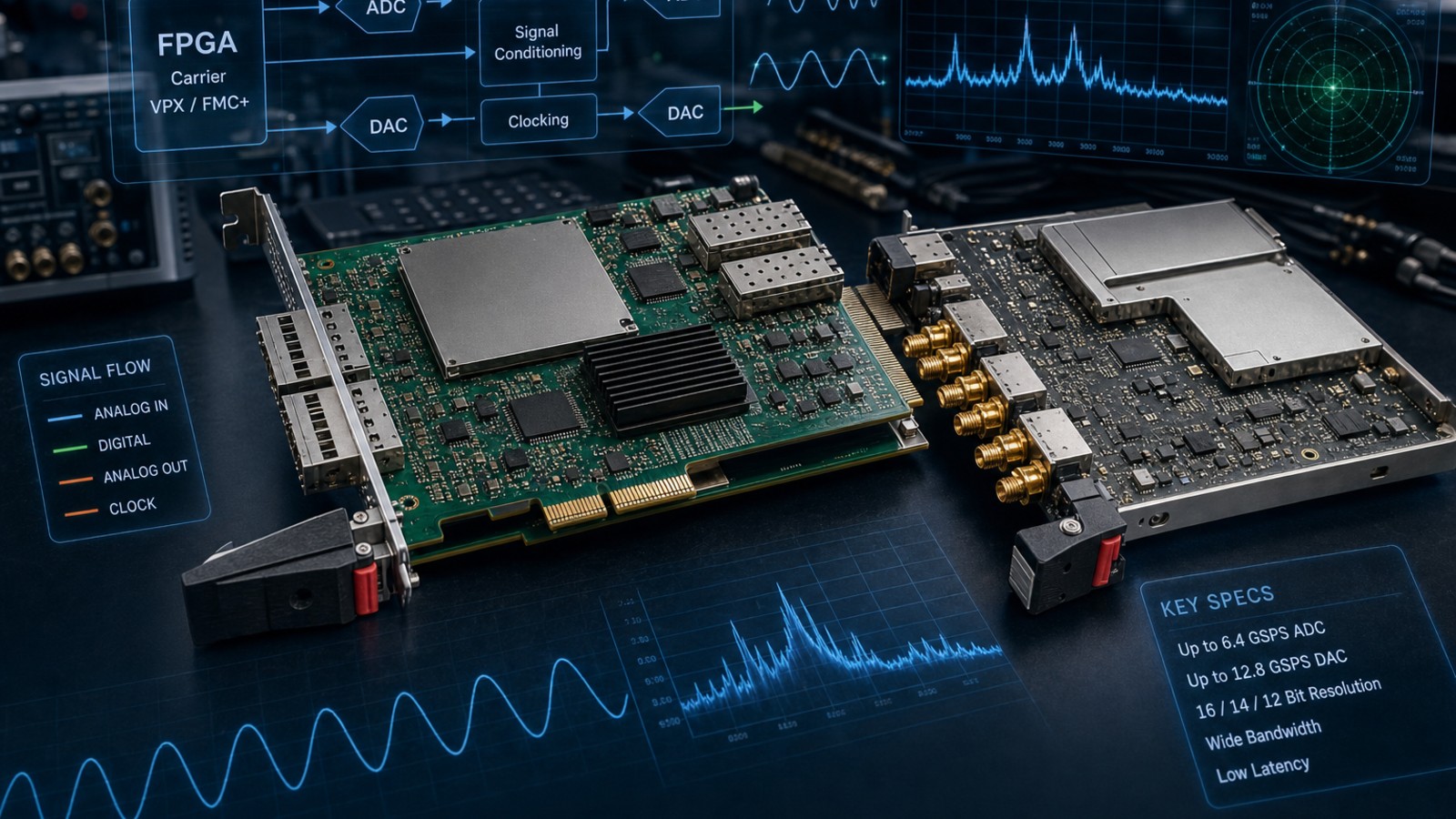
- Application:EW & Radar Applications
- Compliance:VPX Compliant
- MxFE:AD9082 MxFE
- Interface:JESD204B/C
The module pair consists of the following components:
- FPGA Carrier Card — digital signal processing and high-speed data bus
- FMC+ / AD9082 MxFE Card — analog/RF output chain (connected to carrier via FMC+)
This product group is being developed within the scope of TÜBİTAK 1501 Project No: 3260756, under the project titled ‘Development of an FPGA-Based, SOSA- and VPX-Compliant Modular Digital Signal Generator Unit for Next-Generation Electronic Warfare Systems’.
Module components
Two-board architecture
The carrier card handles DTK/IQ processing and JESD data bus; the MxFE card provides analog/RF conversion.
- FPGA Carrier Board — digital signal processing
- VPX and SOSA compatible modular architecture
- FMC+ / AD9082 MxFE Board — analog/RF output
- JESD204B/C high-speed interconnect
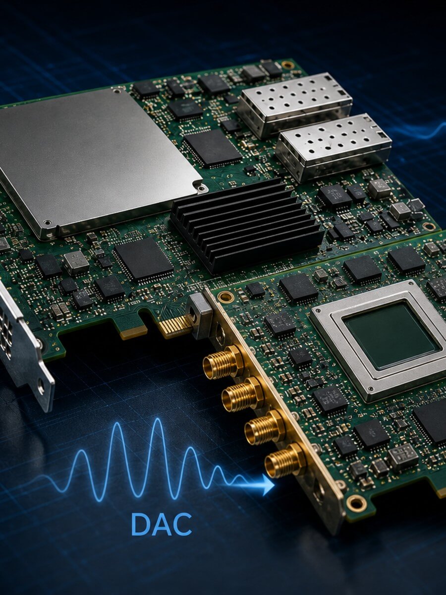
Conclusion
Modular digital signal generator
The FPGA + ADC/DAC module pair provides a VPX-compliant, scalable signal generation platform for electronic warfare and radar applications.